Large Scale Central

My first circuit board

Some of you are aware that, for some time, I’ve been messing with designs for a more robust electric-op switch machine. Inspired by Dave Bodnar’s custom-made boards, about a year ago I turned up the heat on the project. I did the 3D design work in Solidworks and the 2D schematic in Autocad (actually I switched to BricsCad, but that’s another story).

Anyway, the road to getting a circuit board made from mechanical design software has been perplexing, because the board manufacturers take “Gerber” (or similar) design files that are generated by electronics software and those folks that are into that. I’m not electronically proficient, nor do I want to spend gobs of money for specialized software. So, to cut to the chase, here’s the process I’ve gradually settled on.

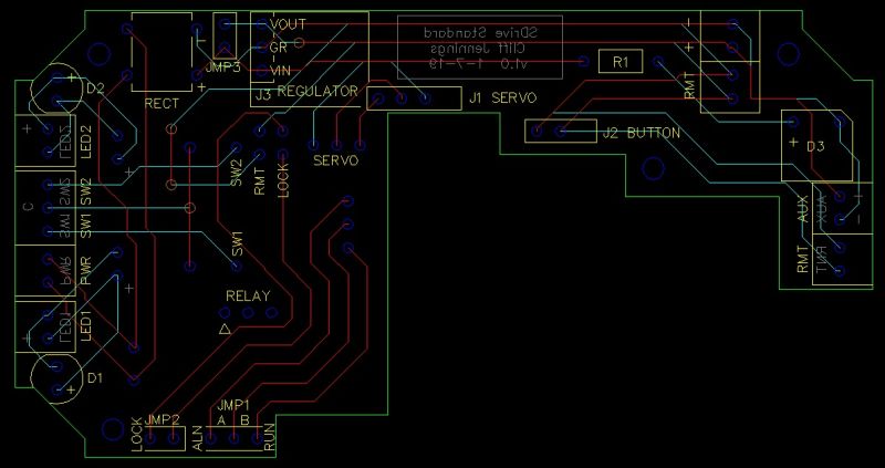
The 3D design, and all “trace” routing, was done in Solidworks. Blue lines are top traces, red are on the bottom. You don’t need to use 3D CAD, 2D is fine; but this is how I wanted to do it, because the packaging is so tight.

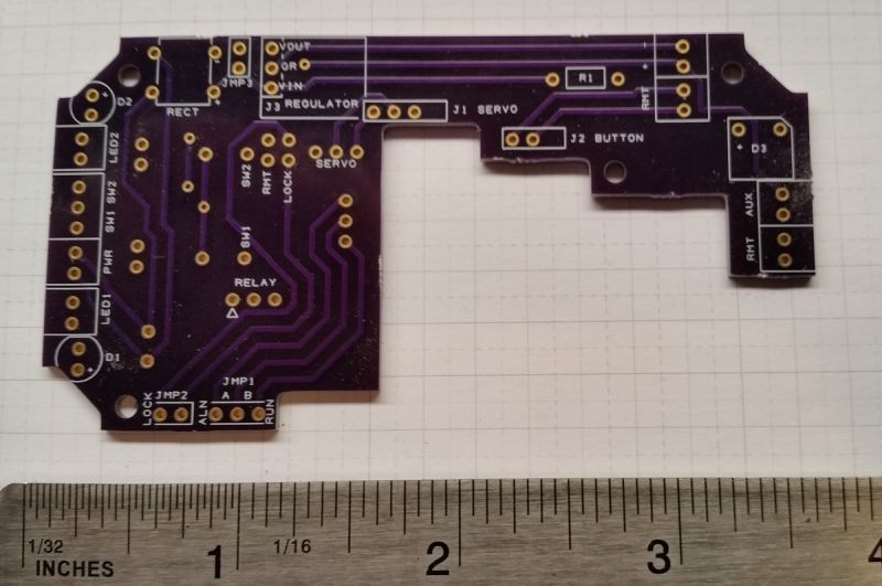
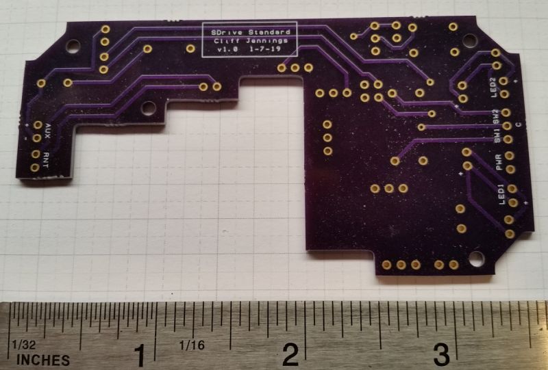
Here’s just the board.

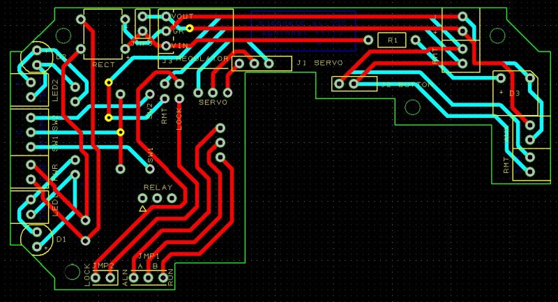
The linework for the board’s outline, holes and traces was exported in a couple views (to keep the top and bottom traces separate. Here’s one of them.

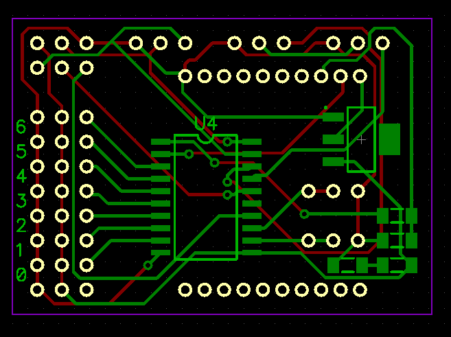
After that came the 2D CAD, using a (very good, but vastly cheaper) Acad clone. I moved things to the proper layers, added text, etc. Reversed gray text will be printed on the bottom side.

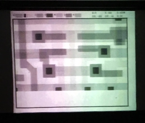
This was exported to DXF format (which looks the same), to get sucked into the sparky software. It took quite a while to get the CAD layer names right, so that they were honored in the next phase. But once that was straightened out, along with a bunch of other misc settings, the import to DesignSpark has gotten very fast. The image below is exactly how it was imported, with the exception of all the round “pads” which had to be manually placed (not very hard though).

DesignSpark offers many products, including this PCB software; and it’s 100% free. This was the key step for me to translate the CAD layers into the “Gerber” or whatever numeric language that PCB manufacturers require. So the last step (and I’ve been trial-and-erroring this all day, but It’s now working great) is to output those files. These files represent all the layers involved, with this list being an example:

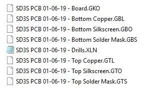
These names are NOT how DS exports them, but how the next step requires them to be named. So after renaming to what you see, the files were zipped into 1 zip file and uploaded to the manufacturer’s site. In this case, and at the advice of Dave Bodnar and others, I’m using Osh Park (Oshpark.com). Again, it took some fiddling around, but the great thing about OP is that they show you how each layer (outline, holes, copper, mask, silkscreen) will turn out before you put the order in. Eventually, all looked ok.

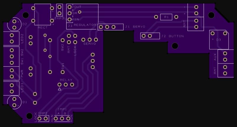
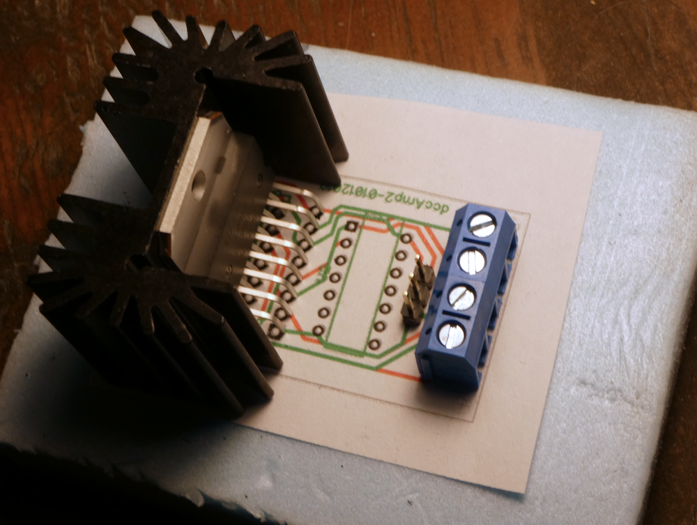
Their prototype service is $5 / sq inch for 3 boards. So, for $35, I’ll get 3 of these to check out. The ultimate objective will be a bunch of these:

Cheers,

===>Cliffy

Sounds like this has been a pain, Cliff. Do you have a schematic? Looks like mostly a relay and a few discrete parts driving a servo? Or is there more to it? This going to be for your switches? You planning to wire up to DCC somehow? Or some switches somewhere central or what? I guess I’m missing the big picture…

Looks complicated, but I’m glad you figured it out. I’ve thought about trying etching services for some photo etching and while it’s not quite as complex as this, it involves multiple steps. Now I know who I can bug when/if I ever get to that project. (https://www.largescalecentral.com/externals/tinymce/plugins/emoticons/img/smiley-wink.gif)

Craig,

A couple of PCB softwares I am aware of are Pad2Pad and PCBExpress. Both are free downloadable softwares that will work great. PCBExpress is a proprietary software for a ‘prototyping’ board manufacturer. Works good and they are pretty reasonable on the boards. One of the members here has used them, and one of our (now going for a PhD) engineers used them frequently.

Pad2Pad I recently downloaded to experiment with, but have not had time to give personal experience. Has been recommended by a couple spark jockies I know and is supposed to be easy to learn. I also believe they said that P2P will output Gerber files.

FWIW

Bob,

How would those work for a etching service? I’m not etching a PCB, but rather just plan brass stock. The services I have looked at want vector files? This is way down on my,list of projects.

Jim, yeah, I’m not surprised that the purpose is vauge; I’m holding off on the description of the that, and the whole switch machine, until I can get the design settled and debugging done. For now though, I was just posting on the board process, because I’m happy to finally close that loop. Thanks though for your interest Buddy!

Craig, you bet; If I can be of any help, let me know. Are you creating the board in any kind of CAD software?

Bob, I actually began with P2P and PCBE, but their proprietary nature means you have to manufacture through them. If it was only a few items, that would have been fine. But in case I get to selling a product down the road, I wanted to crack the nut on the generic / standard Gerber file creation process, because that opens the door for really cheap production. DesignSpark basically does what those products do, while keeping the output non-proprietary.

Cliff

Craig, Sorry for the confusion, I was aiming that at the ‘Gerber’ and circuit board design, not paying attention that it was Cliff doing the circuit board.

Cliff, I was not aware that you had already used those products. What we found at the office, for small runs PCBE was pretty cost effective relative to the cost of the software purchasing stand alone software that provides generic Gerber files. I was also not aware that marketing was in the cards. I applaud you doing it ‘the hard way’, way above my pay grade (http://www.largescalecentral.com/externals/tinymce/plugins/emoticons/img/smiley-laughing.gif).

Thanks Bob, yeah, it was hard, but now that the layers and rules and whatever are nailed down, it’s pretty easy.

I just checked with PCBWay, (a Chinese board manufacturer that takes Gerber files). These boards are 92x48mm. And as complicated as they may seem, they are only $1 each (+ shipping) from them.

Again, the key for me here was finding a way to translate .dwg or .dxf CAD linework into industry-standard Gerber. That was enabled by DesignSpark PCB, a freeware board design product.

BUT, it took the entire last weekend, via trial and lots of error, to determine a layer-naming scheme that, when exported from 2d CAD, could be sucked into DS and be automatically transformed into board outline, traces, silkscreen, etc. The only thing that wasn’t automatic was pad (plated / unplated round hole) placement, and that was fairly easy, once I understood what was needed.

If anyone’s interested further, I can elaborate further. (http://www.largescalecentral.com/externals/tinymce/plugins/emoticons/img/smiley-laughing.gif)

Ok, this is totally off topic but, what the heck…

Turns out that one of my best jobs was actually an internship that started a loooong time ago in 1976. I wrote an editor for chip design layout and as part of that generated Gerber files to make masks for chip production. (each of the different patterns below is output as a different Gerber file, similar to your separate wiring layers on a PCB)

I’ll confess I can’t remember any of the specific details, though I vaguely know what the Gerber primitives are (lines, rectangles at any angle, etc.).

Ok, that’s enough of that. Trying to hijack this thread as little as possible…

Very cool, Jim! I wrote graphic programs in lisp for years, for Autocad. Still use those. My big product was related to 2d pipe fittings and routing, and the program filled a 3" binder. But the world went 3D, and so much for that. But I can relate!

I like Bay Area Circuits. The software is free, huge library of components. The auto route and rubber banding is fantastic and they will give you the gerbers if you make an order.

https://bayareacircuits.com/pcb-design-layout-software-for-custom-pcb/

They have been very good to me for small batches of boards. Once you get the hang of the software you can just kinda goof around and make odd incarnations of circuit board thingies. Way fun.

Just thought I would mention them.

Thanks Martin. I’d tried BAC back in the summer, but now I can’t remember what the roadblock was. Anyway, I should get back in touch with them, maybe they’d have better guidance on trace width (vs current), pad diameters, etc. I’ve been having a hard time determining those, so I don’t have much choice but to overdo the widths and therefore clearances.

I’ve had really good results. You can set the trace width before you route, I do that for my power boards. And I shouldn’t say this but I kinda just guess on some things and then test after I get the board.

One thing that has really helped me is that you can print out a 1 to 1 image on your printer and then see how the components fit and line up before you order a batch of PCBs. That has saved my bacon a few times.

Cliff,

When I get to a etch project (thinking steps for a GP) I will do the 3D design in CAD, then try and convert to a vector file.

I got the boards in from Osh Park yesterday, and am quite pleased with how they look.

Cliff

The first picture - this is the front of the board and there are two terminals at the bottom right corner labeled RMT.

The second picture - this is the back of the same board and those two terminals are labeled RNT.

Tom

Nice! Cool you get them in purple like that. Be sure to post up a pic when you get them populated.

Nice looking boards. I like OshPark for small runs. There are a number of fab houses in China that will do jobs for you too and you can pick your board color. I’ve done traditional green, and red so far.

Thanks Tom, I missed that.

Martin, it’s funny, but OP defaults to purple, I guess it’s a brand thing. Thanks, and will do.

Hi Bob, gracias. Yeah, my quote from PCBWay was only about $1 + shipping, and they had color choices as I recall. They don’t have any previsualization or diagnostic tools like OP, but the price is great (once the bugs and typos are wrung out!).