Large Scale Central

custom circuit boards

OK, I’m no electrical engineer, but I’ve finally been making progress on an electronics puzzle that’s been nagging me for some time. So for better or worse, I want to share what I’ve learned.

I’ve had a switch machine project on the burner for a couple years, and the prototype worked fine. Even brought it to the D&B. But I needed to miniaturize it, and got stuck on the circuit card.

Dave Bodnar’s boards are beautiful; and he told me he used PCBWay.com. Thanks Dave for all your tips!!!

However, I’m a mechanical guy, working in a 3D CAD package (solidworks) and AutoCAD. And I’ve learned that PCB (printed circuit board) manufacturers only accept proper electrical engineering PCB (“Gerber” or similar) files to do their thing. I’ve also learned that professional packages are either very tough to learn (for a non-sparky), or expensive, or both.

Now, I can make DXF files all day long, but no manufacturers accept them. And I didn’t know why. But several board makers, that supply their own version of PCB design, do accept DXF as “footprints” for the board. That is, borders and holes. Unfortunately, the output is proprietary, and you pay through the nose for that particular service.

This post is about how I was finally able to bridge that gap.

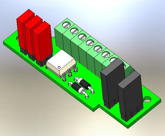
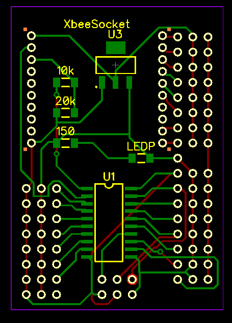
First off, my board is highly bounded by the surrounding geometry, and packaging the components hasn’t been easy.

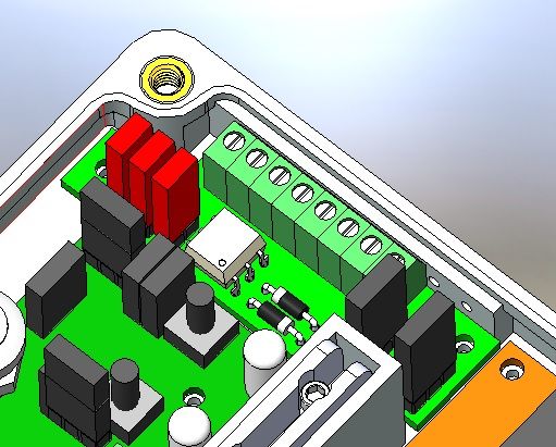
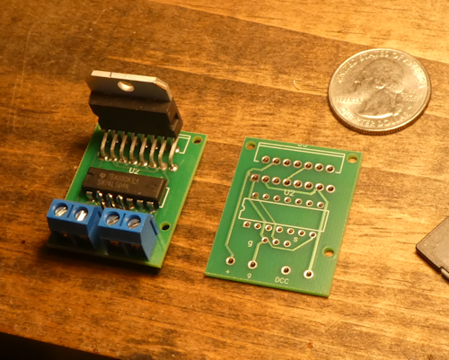
The circuit is simple, and the board is mainly power distribution with a little signal wiring thrown in. Here’s the populated board.

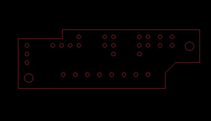
The easy step was to export the board’s geometry to a DXF file.

I hunted for software that accepted DXF, and installed and tested it, only to find that the format was proprietary, the board expensive, and the output wasn’t the Gerber industry standard. So I couldn’t use PCBWay, or sources like that.

But after several gyrations of this, I finally found the key: DesignSpark. DesignSpark PCB is FREE. You have to register, but that’s all. It imports DXF for board footprints, and exports to the industry standard formats.

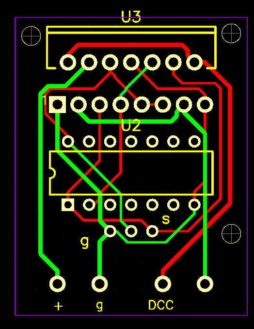
Here’s the PCB design after importing my DXF, converting it into a “board,” parking the “pads” on it and running the “traces”. I’m over-using the quotes here, because these are the kinds of terms I’ve had to become familiarized with.

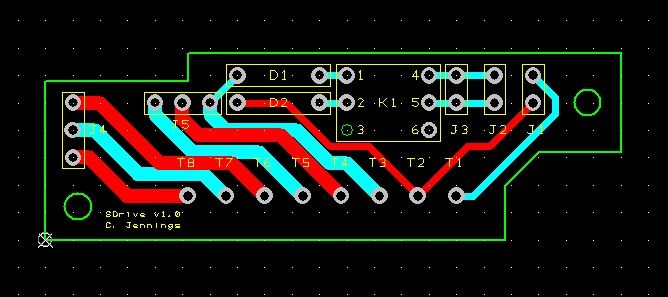
The export function of this software generates the many industry-standard files required for a PCB. For example:

  • Top documentation (the board, in green here)
  • Top copper (topside conductors, shown in red)
  • Bottom copper (bottomside conductors, shown in blue)
  • Top silkscreen (what’s printed; in yellow here)
  • Top copper resist (not shown; automatic; all that green stuff)
  • Bottom copper resist (ditto, on the bottom side)

That’s why DXF or similar CAD files won’t work for this: the layers are in different files, with their own metadata requirements.

All these files are zipped and uploaded to PCBWay. A few 24-hour cycles have passed, while they (in China) found my flaws and told me about them. I fixed, and re-uploaded. And the board is finally passing!

I’m not ready to order quite yet, because I want to breadboard some other stuff and do more testing. But this run-through is telling me that these PCB’s can be had for around 80 cents each, plus S&H of around $9 via “e-packet”.

Probably not gonna rock the socks of a lot of people here, but as a geek I was too excited not to share.

Finally, you folks who do know all about these sorts of things, please share your insights and improvements to all the above!

===>Cliffy

Clif - nice project and well explained for those who need to design as you did.

If you want to save a few $$$ you can get prototype boards for only $2 + shipping - I have used their services and the boards are A-1 - they accept the same Gerber files as other firms

https://jlcpcb.com/

Be sure to let us know how the rest of the project goes

dave

I use DesignSpark Mechanical for my 2D and 3D CAD files. It too is fairly easy to use and free.

Have you tried designing in ExpressSCH and pricing in ExpressPCB? That’s what I use for electronic design (free), but have never used their service to produce the board.

https://www.expresspcb.com/expresssch/

I’ve had PCBWay and ShenZhen2U make boards for me. And also used OSH Park. All top quality and my ShenZhen2U order I placed on a Frida, they were shipped Monday and I got them Thursday. OSH Park is neat for one-offs.

I use https://bayareacircuits.com/ I like the free pcb design software they have. Great autorouting.

Thanks for all the additional ideas guys!

Before trying Designspark, I worked the board up in Pad2Pad, but their files were proprietary, and a single board was over $200. A run of 20 or 30 wasn’t much more, but the setup was way high. With the standard Gerber files in hand, I’m getting a price of 50 cents now from PCBWay.

But shipping isn’t always cheap or quick, so I’m doing a little comparison on those.

Source Qty Price Shipping Co. and working days to ship

JLPCB 10 $5 $19.60 DHL, 3-5

JLPCB 10 $5 $12.62 Air mail, 15-20

PCBWay 10 $5 $21.00 DHL, 3-5

PCBWay 10 $5 $7.00 E-packet, 10-15

shenzhen2u 10 $10 $23.63 DHL, 3-8

shenzhen2u 10 $10 $7.00 China post, 8-21

I’m working on a quote from OSH Park, they didn’t like my board layer file.

Having a couple problems though, and I can’t find the answers in the DS help.

DS didn’t export any dedicated file for the board outline; but a file called “top documentation” has it in there. OSH Park’s reviewer didn’t like that.

What’s the standard way to name a Gerber board outline file?

And can it have any mounting holes in it?

Cliff

I found a neat tool to view zipped Gerber files with, layer by layer:

http://www.gerber-viewer.com/

Bob, you’re right, OSH Park is really neat. Their layer-by-layer on line proofing is amazing, shows your board with each layer fully explained. And $7 for 3 boards, 5 working ways, free shipping – hoddayam!

Support is great, in the last hour I’ve emailed them twice and gotten replies for both.

Trying BAC next.

[edit] In an email reply, they said use their 2-layer special. But, it costs $30 x 3, yep, $90. So negatory on that. Martin, did you have a different experience?

Todd Brody said:

I use DesignSpark Mechanical for my 2D and 3D CAD files. It too is fairly easy to use and free.

Have you tried designing in ExpressSCH and pricing in ExpressPCB? That’s what I use for electronic design (free), but have never used their service to produce the board.

https://www.expresspcb.com/expresssch/

Todd, good to know, thanks!

I’ve not used the Express products. [edit] But I just went to their site, and saw this info:

  • Standard MiniBoards are 2 layer PCBs without the solder mask or silkscreen layers. [huh, all the other services had those important elements…]
  • For a fixed price of $51, you will receive 3 identical boards.
  • The board’s size must be 3.8 x 2.5 inches. [not sure if that’s a max, or a must-be outline?]
  • Orders submitted Monday through Friday by 2:00pm ET are shipped the next business day.

That’s definitely a great turnaround. But OSH Park’s $7 (even if faster shipping is chosen) really spanks that $51.

FWIW, I’m leaning toward OSHP for proto, and PCBW for the main run (I need around 20 or 30).

Thanks again Dave B and everyone for helping me puzzle through this.

Cliff

Cliff:

In San Diego, most professional houses use PADS, (besides my little company, Qualcomm uses it too) by Mentor Graphics. Of course it’s thousands of dollars, and handles complex products, our current board is 12 layers with several power planes and different materials for making different impedance traces working at different frequencies.

But there is supposedly a free version called PADS Maker, and it is a dumbed down version of this professional system, so making footprints (you called them outlines) and routing, and vias and everything is in it of course.

This package is used worldwide and accepted by every PCB manufacturer, of course you export Gerber files most times, and these are mostly driven by the schematic, not starting from mechanical CAD.

I’ll investigate further, because it should make the process easier, and never a problem with compatibility.

(also if you get stuck, I can have my h/w engineers and/or layout guys help)

I know you aren’t making anything complex… yet! My opinion is if the learning curve is not horrible, I’d rather drive a detuned Ferrari than a hopped up Volkswagen if you get the analogy.

Greg

Cliff, sorry, didn’t mean to mislead you if I did. I’ve been using BAC for a while but I do everything in their software. They will give you the gerbers if you do an order but I have not had a need for them. I did use Pad2Pad before this but they were way more expensive so I tried these guys. Mostly I wanted easy to use software that has a good auto-route. Theirs is very good IMHO. The s/w has a small learning curve but my needs were simple so it wasn’t bad at all. I even made a custom component for the Xbee socket with it’s odd pin spacing.

Here is one of my older Xbee ATtiny boards- this one obviously is more digital, no real loads here and several SOIC components.

I just loaded this one up in their software and pressed ‘order’. Came to $6.47 each for qty 10 (10 day turnaround). (100 is $4.20 per board for reference)

This one is more analog, it’s $2.30 for 10.

Here is that board, naked and also populated. It’s not very big but I’m very happy with the quality and they work very well once everything is soldered up.

Greg, thanks for the info! And if PADS Maker can import DXF for footprints, it’s certainly worth looking into. I sure hadn’t heard of it, thanks. [edit: I couldn’t find that it imports DXF, but that won’t be a problem for most folks I expect].

DesignSpark PCB appears to be doing OK – except for some quirky Gerber default file naming, which I think I’ve resolved now. Seems to handle some fairly complex and multi-level boards. Thanks for thinking I’d want to (or be able to) tackle more than 2 layers in the future… my brain hurts just thinking about it though… (http://www.largescalecentral.com/externals/tinymce/plugins/emoticons/img/smiley-foot-in-mouth.gif)(http://www.largescalecentral.com/externals/tinymce/plugins/emoticons/img/smiley-laughing.gif)

Martin, thanks for the pics and backstory, great design work. All auto-routed, huh? I had to manually place my traces, and that was a bit of a challenge even on my tiny board (by the time I complied with all the rules).

That’s a nice looking board. Were they $2.30 each, or for the lot of 10? Either way, peanuts!

Thanks guys, this is all a lot of fun!

Cliff

Ouch, sorry, missed that one, yeah $2.30 each in lots of 10. This one you don’t save much for lots of 100, $2.06 each. Guess because it’s so small.

Yep, all auto routed. I do love that feature. I don’t think I could do these boards without it. You just connect the pins with ‘fly wires’ then click the button and presto. Very slick.

I ‘fattened up’ the traces for the power after the auto route. Worked great.

Cliff, I will check, but I believe you can do the footprints in PADS itself, and build your library of parts. Also, you can probably “find” libraries of standard parts and connectors to save time.

Greg

Very cool, Martin. DesignSpark also has that (they call it “Nets”). I gave it a cursory try, but I didn’t have the patience to make it work. That’s pretty impressive routing though, I need to revisit that.

Thanks Greg, that would be helpful for folks who don’t need the dxf importing. It’s great that we can gather a bunch of options in this thread, for others in a similar situation. And PADS Maker sure looks like a great tool.